In today’s ever-evolving technological landscape, the application of laser technology in modern manufacturing is steadily maturing. A diverse range of processing techniques has ushered in greater innovation within the manufacturing sector. Laser technology continues to advance, evolving from its previous nanosecond iterations to its current picosecond and femtosecond levels. The emergence of infrared picosecond laser marking for metal has provided reliable solutions for the micro fabrication field. Its unique processing characteristics find extensive application across various micro fabrication domains.
Ultra-short Laser Marking: What Are Nanosecond, Picosecond, and Femtosecond?
In laser processing, the unit of time control refers to the operation of applying single-pulse energy to a material’s surface in an extremely short time frame. This high-frequency repetitive operation can be used for various applications such as drilling, cutting, marking, welding, and more. It’s important to note that time units can be converted into different measurements: 1 second equals 10^9 nanoseconds, 10^12 picoseconds, and 10^15 femtoseconds. Therefore, nanosecond, picosecond, and femtosecond laser marking devices are named based on these time units. The shorter the time, the less impact the laser has on the material’s surface, resulting in better processing outcomes.
Depending on the processing requirements of different materials, one can choose the appropriate industrial laser marking equipment. For instance, nanosecond laser cutting machines are commonly used for processing thin-film materials, while femtosecond laser cutting machines are preferred for brittle material processing and conductive thin-film oxide materials.
What are the Advantages of Pico-second Laser Marking Machine?
Today, micro fabrication typically involves handling micron-level details such as holes and slots while minimizing heat damage to surrounding materials during the process. This means that precise and clear incisions need to be achieved with minimal impact on the thermal characteristics of the surrounding areas.
In the early stages, due to the immaturity of picosecond laser technology, it often came with high costs. However, modern picosecond laser devices have virtually no heat-affected zones and offer wide applicability, making them a staple in modern micro fabrication.
The suitability of picosecond laser machining for the modern micro fabrication industry primarily stems from their ability to directly break the bonding of target materials using laser photons. This is considered a “cold” processing method, with minimal to no heat-affected zones.
Additionally, the entire process is exceptionally clean and avoids issues related to solidified materials. As a result, modern picosecond laser machine, such as picosecond laser marking machines and picosecond laser cutting machines, are widely applied in various aspects of the micro fabrication industry. These unique performance characteristics inject new vitality into the modern micro fabrication industry.
Nanosecond VS Picosecond Black Laser Marking
Due to the partial heating of the marking surface with long nanosecond pulses, such as edge protrusions, melting, debris, substrate cracking, or damage, various problems can arise. Utilizing a picosecond laser engraving machine enables high-speed, high-quality, fine marking on components related to mobile and related products. Picosecond laser marking machines have extremely short interaction times, with almost all the energy being directly applied to the mobile device components, resulting in instantaneous laser ablation and high processing efficiency.
Picosecond laser marking machines can be widely applied to thin materials, ceramic drilling and marking, ink removal, coating removal, plastic materials, micro and invisible marking, precise cutting of thin-film materials, and marking. They have a focal spot diameter as small as 0.01mm, characters as fine as 0.05mm, and are characterized by narrow pulse widths and high peak power, resulting in very fine marking effects. They are applied in industries that require high precision marking, as well as in the processing of brittle materials and offer excellent anti-counterfeiting effects and resistance to etching and oxidation. They are widely used in the medical equipment, medical supplies, surgical instruments, precision automotive components, electronic components, mold engraving, and chip industries, among others.

Stainless Steel Black Marking with Picosecond Lasers
The demand for stainless steel surface information marking, particularly black markings, is rapidly growing. Traditional methods like painting and silk-screen printing have issues such as paint chipping and delamination. Heat transfer printing fades with time, and chemical etching and steel stamping cannot achieve the desired black marking effect and have other inapplicable issues.
In contrast, picosecond marking technology is a non-contact process that does not harm the workpiece. It offers non-toxicity, environmental friendliness, flexibility in content, and permanent marking, with these features being particularly prominent in the medical equipment industry, making laser marking the preferred choice.
Stainless steel typically has a silver-white appearance, and laser-marked coloring preserves its excellent properties, expanding its usability. In laser marking, the principle of achieving black markings differs between nanosecond and ultrafast laser technologies. Nanosecond lasers typically produce colored oxides, including black, whereas picosecond laser marking create a visual black effect through the generation of non-reflective nanostructures.
In practical applications of laser coloring on stainless steel, achieving the desired color can be challenging. Black, as well as different colors, can be generated by adjusting parameters such as frequency, pulse width, and defocus. Under certain parameter settings, color variations may occur with changes in the laser source, scanning mirrors, and focusing optics.
For applications with high requirements for black marking on stainless steel and significant process demands, laser technology has gradually replaced traditional marking methods. To ensure better quality assurance, using picosecond pulse lasers for black marking on stainless steel is currently the preferred choice. Laser technology, with its unique capabilities and efficiency, is poised for wider development and application in the medical industry.
Application of Picosecond Laser Glass Marking
Laser marking can rapidly and clearly mark text, symbols, and patterns, with character sizes ranging from millimeters to micrometers, which holds special significance for the anti-counterfeiting of product QR codes.
Due to the brittle nature of glass and its high light transmittance, continuous wave lasers or long-pulse lasers can make it difficult to produce clear and aesthetically pleasing patterns and markings on glass due to heat accumulation.
Laser marking is a method of marking that uses a high-energy density laser beam to irradiate a localized surface of a workpiece, causing rapid vaporization or color change of the surface material, resulting in a permanent mark. As an essential component of automobiles, advanced picosecond laser marking technology has significantly improved production efficiency and enhanced anti-counterfeiting capabilities in the manufacturing of car glass.

Picosecond laser marking uses high-power density laser photons to directly break the bonding of the target material, causing it to instantly reach a plasma state and be rapidly removed. This process generates almost no heat-affected zone. Since laser marking is a non-contact process, it is highly friendly to car glass materials, avoiding issues like cracking, and it requires no post-processing. This technology provides an efficient and sustainable means of adding identification and anti-counterfeiting elements to car glass.
Picosecond Laser PCB Marking
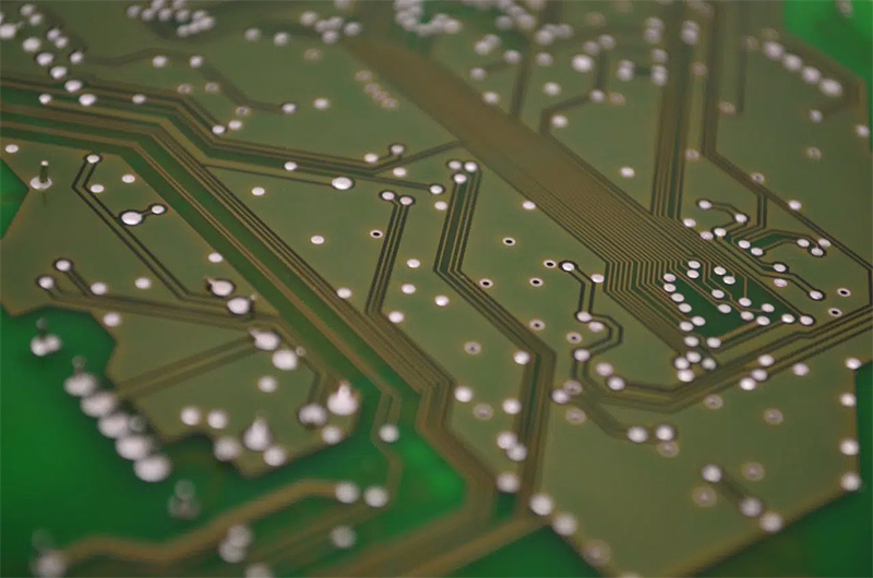
In order to connect electronic components on a circuit board, it is often necessary to create tens of thousands of micrometer-sized small holes on the circuit board. Therefore, ensuring that no heat input affects the stability of the substrate during the drilling process is of paramount importance, and picosecond laser marking system are the ideal tool for such applications.
Picosecond lasers can process holes through an ablation drilling method and offer significant flexibility in terms of shape and size while ensuring the uniformity of the holes. In addition to circuit boards, picosecond lasers can also drill high-quality holes in various materials such as plastic films, semiconductors, metal films, and sapphire.
Picosecond Laser Wafers Cutting and Drilling
The application of infrared picosecond laser marking machines in cutting drilling semiconductor wafers involves the precise and efficient cutting of these wafers using high-energy, ultra-short pulses of infrared picosecond laser beams. the application of infrared picosecond laser marking machines in cutting semiconductor wafers is revolutionizing the semiconductor manufacturing process by providing a high-precision, efficient, and low-thermal-impact solution for creating intricate patterns and structures on these essential components of modern electronics.

Infrared and Blue Pico Laser Marking
Blue laser engraving and red laser engraving are two popular forms of laser engraving. Blue laser utilizes a shorter wavelength (400-450 nanometers), enabling higher resolution and precision, making it suitable for applications that require high-precision detail engraving. It can create a smaller focus, resulting in clearer details. Blue pico laser marking is typically used for engraving various hard materials such as metals and ceramics.
Red laser, with its relatively longer wavelength (635-680 nanometers), exhibits stronger heat scattering and absorption, making it suitable for engraving heat-sensitive materials like soft rubber, plastics, and paper. Red laser also offers higher transmission efficiency, allowing for better penetration into the material for engraving.
DPLASER Infrared Picosecond Laser Marking & Engraving Machine
Pico-second laser marking equipment is used for high-precision and high-quality marking and engraving on a variety of materials, including metals, plastics, ceramics, and more. They are known for their extremely short pulse durations in the picosecond range, which allows for minimal heat transfer to the surrounding material. This results in precise and clean markings with minimal risk of damage or discoloration.
1. Adjustable laser repetition frequency (50kHz-4000kHz), high laser peak power, TEM00 mode output, ultra-short pulse width (<15ps), fast scanning. Used for micro processing of brittle materials such as glass, sapphire, ceramics, etc.
2. Ultra-precise marking on glass materials, fine marking of small hidden QR codes (0.2mm*0.2mm), and other intricate markings.
3. Processing on metal medical instruments with traceability markings that provide acid resistance and oxidation resistance.
4. Cutting and drilling on plastics, oxides, and organic materials, or removal of surface coatings.
5. Logo marking on high-end electronic products.
6. It enables precise shaping of super hard materials.
7. Substituting chemical etching for deep processing on metal materials.
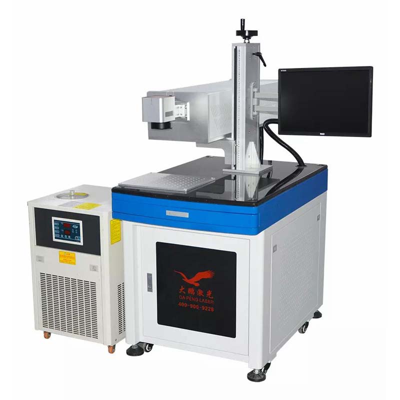
Infrared picosecond laser marking machines are indeed used for precision cutting of various materials, including silicon and compound semiconductor wafers. It offers advantages in terms of precision, minimal thermal damage, and clean processing, making it a valuable tool in semiconductor manufacturing and other high-precision applications.
Summary:
From nanosecond vs picosecond black laser marking, we can see that the differences between laser applications. Its application performs differently in different materials and requirements. As laser technology continues to mature, laser equipment is offering innovative solutions for various industries. Among these, infrared picosecond laser marking has emerged as a versatile and powerful tool, driving advancements in precision marking and precision machining. In summary, the ongoing improve and diversification of infrared picosecond laser marking machine have significantly expanded its applications across industries, promising higher levels of efficiency, precision, and innovation in the future.

