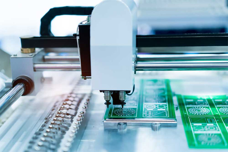
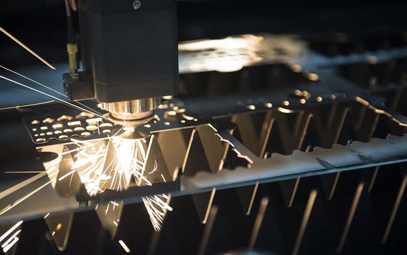
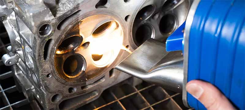
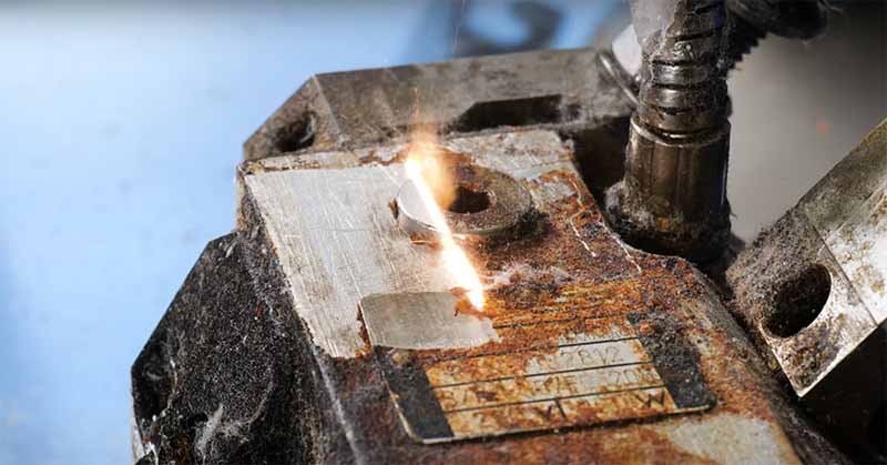
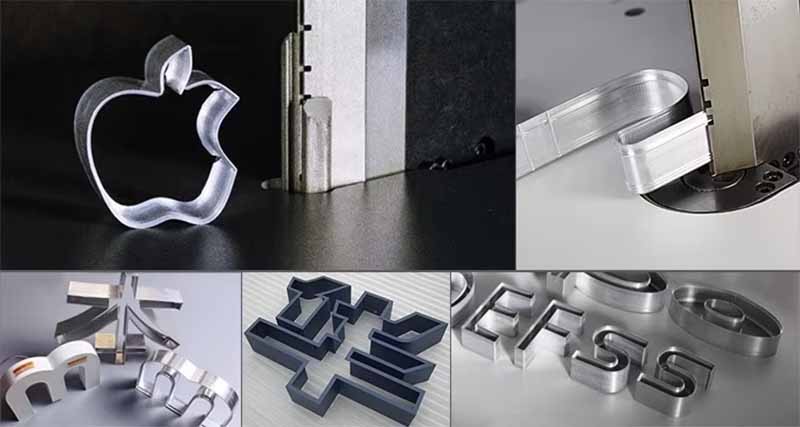
The PCB (Printed Circuit Board) consists of an insulating substrate, conductive traces, and pads, and is used to connect and support electronic components. It is widely used in various industries, including consumer electronics, automotive electronics, and telecommunications, medical, military, and aerospace. With the rapid development of electronic products and automotive electronics, the demand for PCBs continues to grow. As the PCB industry moves toward lighter, more integrated, and higher-precision designs, traditional cutting processes face challenges such as edge burrs, dust, stress, and wear. In contrast, laser cutting PCB machine offers several advantages, including non-contact processing, stress-free operation, no dust, smooth and burr-free edges, and the ability to handle complex patterns and PCBs with mounted components, making it a superior choice.
Why does PCB Need to be Cut?
In order to better meet the needs of different applications, PCB cutting plays an important role in the design and production process, and the following are the two main cutting needs.
- Custom Size: Standard PCBs may not fit the specific dimensions required for a particular project or enclosure. Cutting allows the PCB to be adjusted to the appropriate size, ensuring a perfect fit.
- Penalization and Separation: During manufacturing, PCBs are often produced in larger panels, and cutting (or depanelization) is necessary to separate individual boards for final use. This allows multiple PCBs to be fabricated together in a more efficient process, saving costs before cutting.
Can You Cut PCB with Laser
Yes, PCBs can be cut with lasers, and laser cutting is increasingly popular for PCB manufacturing due to its precision and flexibility.
Of course, traditional PCB depaneling methods also offer a variety of options. Each method has its unique advantages, and selecting the right one can effectively enhance production efficiency and product quality. By understanding these different cutting techniques, you can choose the most suitable process based on the specific design requirements and production scale of the PCB.
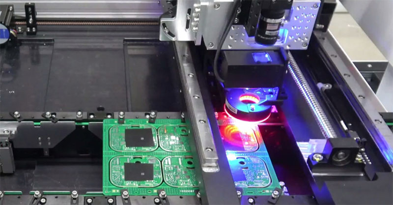
Laser Cutting PCB:UV lasers or CO2 laser cutting machine can cut PCBs, making them particularly suitable for high-precision, complex, and intricate designs. This method also minimizes stress and thermal impact on the material.
CNC Milling Routing: Using a CNC (Computer Numerical Control) milling machine with specialized tools, this method is ideal for cutting complex shapes and producing prototypes or small batches of PCBs.
Drilling: Drilling holes in the PCB and separating the material along predefined paths is a simple method suitable for small or less complex PCBs.
V-Cut: A V-shaped cutting tool is used to carve along predefined paths, making this method highly efficient for large-scale production and high-volume PCB depaneling.
Mechanical Punching: This method involves using a punching machine to quickly cut through thinner PCBs, offering fast and cost-effective processing for large quantities.
What are the Applications of Laser Cutting Printed Circuit Board?
Laser Cutting in PCB Industry
- PCB Cutting: Laser cutting uses high energy and precision to create fine, complex shapes on PCBs, ensuring clean edges and accurate routing of the circuit traces.
- Metal Drilling and Cutting: For PCBs that require drilling, laser cutting can quickly and accurately perforate the material, without causing damage to the surrounding areas. This makes it an ideal solution for precise hole creation in sensitive or high-density circuit designs.
In the PCB industry, the use of laser cutting machines has significantly enhanced production efficiency and reduced labor costs. The high precision of laser cutting minimizes material waste to the greatest extent. It also offers high efficiency and accuracy, making it a superior choice over traditional methods like blade cutting, milling, and routing, which often generate dust, burrs, and may apply stress to the board—especially for small or component-mounted PCBs, where the impact can be substantial.
Advantages of Laser Cutting PCB
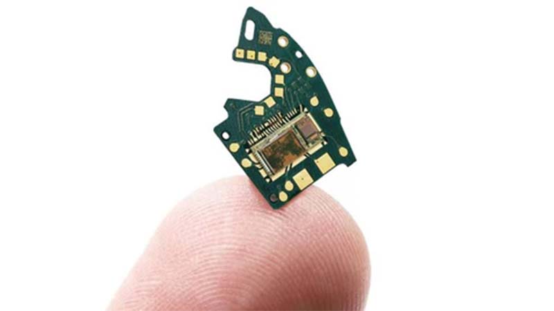
Non-contact Cutting: Laser cutting uses a non-contact processing method, avoiding physical pressure on the PCB. This prevents damage caused by mechanical stress, ensuring that the PCB remains intact, especially for sensitive or small designs.
High Precision: Laser cutting offers tolerances down to a few microns. CNC laser systems ensure high accuracy and fine processing capabilities, making it ideal for the manufacturing of tiny circuit boards while maintaining product precision and stability.
High Efficiency: Laser cutting operates at high speed and with strong continuity, making it suitable for mass production. It does not require complex tooling, greatly reducing the time needed for PCB prototyping, which is especially beneficial during the early stages of product development.
Versatility: Whether cutting simple or complex patterns, lasers can handle a wide variety of designs, including single-layer, multi-layer, flexible, and complex PCBs, providing flexibility in production.
Minimal Heat-Affected Zone (HAZ): The heat generated during laser cutting is concentrated in a very small area, effectively protecting surrounding materials from thermal damage.
No Dust, No Burrs: Laser cutting is highly precise and almost eliminates the generation of burrs or jagged edges, making it ideal for the production of high-precision electronic products.
Material Versatility: Laser cutting machines can process a wide range of materials, from standard FR4 to flexible polyimide films. They support various PCB designs, including rigid, flexible, and rigid-flex boards, without needing to switch equipment, thus meeting diverse production requirements.
In summary, laser cutting provides a highly effective, precise, and flexible solution for PCB manufacturing, offering significant advantages over traditional methods, especially for complex designs and high-precision applications.
PCB Laser Drilling
Laser drilling is particularly well-suited for creating micro-holes and blind holes in PCB processing. Compared to traditional mechanical drilling, it can achieve smaller, more precise hole diameters and allows for better control of hole depth. Since laser drilling is a non-contact process, it eliminates the need for frequent tool replacements, reducing maintenance costs and improving production efficiency. Furthermore, this technology is ideal for multilayer designs, helping meet the demand for smaller and higher-density electronic products. Overall, laser drilling plays a crucial role in the miniaturization and precision of modern electronic devices.
Laser Marking PCB
Laser marking is used to engrave identifiers, component placements, or other markings onto the PCB surface. Due to its high resolution and ability to make tiny markings, laser marking is particularly well-suited for PCB production. It allows clear text or barcodes to be marked in confined spaces, ensuring each PCB has a unique identification. This type of marking is clean, permanent, and cost-effective, making it easy to identify PCBs during assembly and ensuring traceability throughout the manufacturing process.
Limitations of Laser Cutting in PCB Manufacturing
High Initial Cost: The purchase and maintenance costs of high-quality laser cutting machines are relatively high. For small manufacturers, this can make laser cutting more expensive than traditional methods, especially in small-batch production.
Material Thickness Limitations: Laser cutting is most effective for thin materials, which is suitable for most PCB applications. However, when dealing with thicker materials, laser cutting may face challenges. For heavy-duty applications or thicker PCBs, traditional processing methods may be more appropriate.
Thermal Effects: While laser cutting minimizes mechanical stress, it still generates heat, which can affect sensitive materials or components on the PCB. The heat-affected zone (HAZ) could cause thermal damage or impact the performance of delicate components, requiring careful control of laser parameters to mitigate these effects.
How to Choose the PCB Laser Cutting Machine?
PCB materials are mainly categorized into two types: rigid substrate materials and flexible substrate materials, with common materials including copper-based boards, aluminum-based boards, fiberglass boards, and epoxy resin boards. The choice of laser cutting machine depends on the type of material to be processed, as different materials require different laser sources.
Metal Substrates (e.g., copper boards, aluminum boards):
For cutting metal-based PCBs, infrared laser cutting machines are typically used. These machines are equipped with focusing heads to facilitate penetration cutting. Additionally, assist gases such as nitrogen, oxygen, argon, or air are often used to help with the cutting process and reduce oxidation or contamination on the material’s surface.
Non-metal Substrates (e.g., epoxy resin boards):
For cutting non-metal PCBs, green light or ultraviolet (UV) laser cutting machines are preferred. These lasers are capable of cutting through materials like epoxy resin boards with high precision and minimal heat-affected zones, making them ideal for delicate, non-metallic substrates.
Pico-second Laser Marking & Engraving Machine
The picosecond laser cutting machine is used for ultra-fine processing tasks such as panel cutting, contour cutting, drilling, and cover-lay cutting. It is primarily applied in the precise cutting, drilling, and marking of materials like FPC (Flexible Printed Circuit), PCB, FR4, and cover-lays.
Features:
- Auto Positioning and Focusing: Achieves high-precision, fine cutting of a wide range of materials through automatic focus adjustment, ensuring optimal results.
- Etching Lines and Micro-hole Processing: Perfect for fine processing tasks, with a vacuum adsorption platform that ensures stability and environmental friendliness during operations.
- Minimal Heat Impact: The cutting edges are smooth and clean, with minimal heat-affected zones, reducing the risk of thermal damage to sensitive materials.
- CCD Dual-Lens Automatic Imaging System: Provides precise visual positioning and real-time monitoring, ensuring accuracy throughout the cutting process.
- High-Precision Components: The machine features imported roller-type guides and grinding-grade ball screws, ensuring high precision, stability, and smooth operation.
This picosecond laser cutting machine offers an advanced solution for precision PCB and FPC manufacturing, capable of handling delicate designs with exceptional accuracy and efficiency.
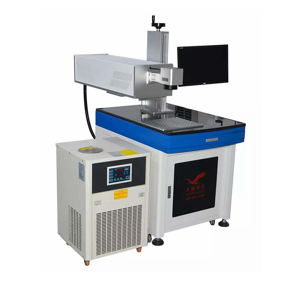
UV Laser Engraving & Cutting Machine for PCB
Using UV lasers to cut PCB (Printed Circuit Boards) offers extremely high processing precision and superior quality. UV lasers, with their shorter wavelength, can achieve fine focusing, resulting in very small heat-affected zones on the material. This minimizes thermal damage to surrounding areas and ensures smoother cutting edges, reducing the need for additional post-processing.
Additionally, since UV lasers are cold light sources, they produce almost no heat during the cutting process, making them ideal for temperature-sensitive materials, such as the electronic components on PCBs.
The intelligent control system automatically recognizes the PCB layout and performs precise cutting, ensuring that each cutting edge meets design specifications. The automated operation reduces manual intervention, significantly improving production efficiency. Furthermore, the high precision reduces rework caused by inaccurate cuts, further lowering production costs.
The standard processing sizes typically range from 400x300mm to 500x400mm, but custom sizes can also be made based on customer needs.
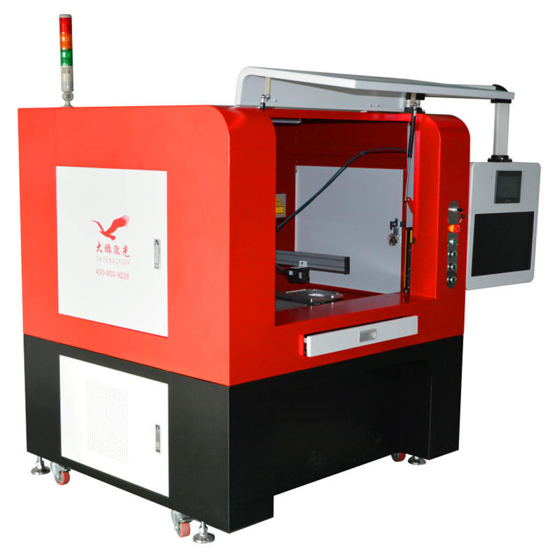
Features:
- Efficient Cutting: Designed for large-area and irregularly shaped circuit boards or thin plates, it can cut both single-layer and multi-layer boards quickly and efficiently.
- High-Quality Laser: Utilizes high-performance CO2 or fiber lasers, providing excellent beam quality, small focus spots, and even power distribution for precise cutting.
- Intelligent Positioning: Equipped with a high-resolution CCD camera, the system automatically locates, identifies, and provides feedback reports to ensure accuracy.
- Stable Structure: The metal housing and compact design ensure stable and precise operation during the cutting process.
- Flexible Adjustment: Features automatic focusing and track width adjustment to meet the demands of different production lines and board sizes.
Applicable Industries:
This PCB precision laser cutting machine is widely used across various industries for cutting different types of PCB substrates, including ceramic boards, rigid-flex PCBs, FR4, FPC, fingerprint recognition modules, cover-lays, composite materials, copper boards, aluminum boards, and more. Its high precision and versatility make it ideal for a wide range of applications in the electronics manufacturing industry.
In conclusion, laser cutting technologies represent the future of PCB manufacturing. With their high precision cutting and engraving capabilities, PCB laser cutting machine achieves exceptional precision, efficiency, and flexibility. They enable the production of more advanced and miniaturized electronic products. As demand for smaller, more complex PCBs grows, laser cutting will continue to play a critical role in shaping the future of electronics manufacturing.
